Impact of disorder in the charge-density-wave state of Pd-intercalated ErTe3 revealed by the electrodynamic response
The interplay between broken-symmetry ground states, either via competition or coexistence, belongs to the mostly explored topics of modern solid-state physics and seems to be an essential ingredient in the arena of strongly correlated materials. It goes without saying that the discovery of a charge-density-wave (CDW) phase in the middle of the pseudogap region of the high-temperature superconducting cuprates (HTC) brought into focus the intrinsic nature of those very different cooperative electronic phenomena, suggesting novel concepts such as intertwined order. Moreover, it is a widespread wisdom of competing orders that the disorder-induced suppression of the CDW state may naturally lead to the increase in the superconducting critical temperature Tc.
Here, we address the Pd-intercalated ErTe3 (from now on also noted as PdxErTe3) at its double CDW phase transitions at TCDW1 and TCDW2, which recently emerged as a model family of materials serving as suitable playground for a controlled tuning of disorder, with the intent to trace its implications from the perspective of the charge dynamics represented here by the real part (σ1(ω)) of the optical conductivity.
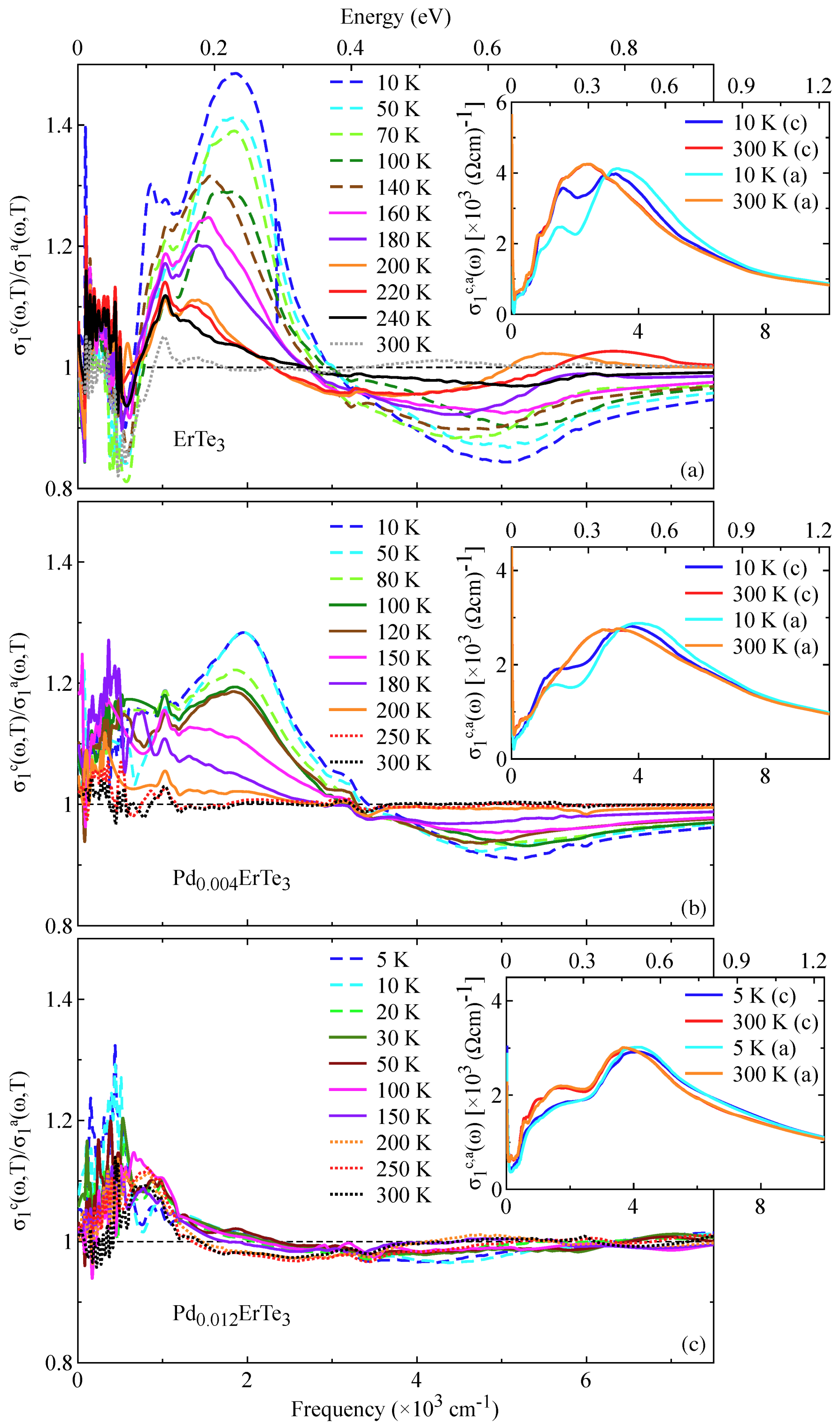
Our collected data (Fig. 3.21) grasp first of all an anisotropic optical response, emerging between the two in-plane crystallographic axes but diminishing with disorder, and second emphasise the relevance of CDW precursor effects, the latter present already at T > TCDW1 and evolving into a long-range CDW order at T < TCDW1 and TCDW2 in the pristine (x = 0) and weakly Pd-intercalated PdxErTe3. Overall, we anticipate that these findings bear testimony to an important reconstruction of the electronic band structure as well as to a substantial spillover effect of the intercalation-driven disorder with respect to both CDW transitions.

In addition, we consider the model-independent analysis based on the integrated spectral weight (SW) and consider the SW ratio with respect to 300 K, given by SWc,a(T)/SWc,a(300 K) and shown as a function of T in Fig. 3.22 for the a (lower panels) and c (upper panels) axis. We clearly reveal that a smaller fraction of the Fermi surface (FS) gets gapped by the CDW transitions upon increasing the Pd-intercalation concentration x. Indeed, the depletion below 1 of the SW ratio itself is a rough measure of that fraction, which is on the order of 10 to 30 % (graphically sketched by the grey areas in Fig. 3.22). Particularly along the a axis, for which the anomalies in the dc resistivity are remarkably more pronounced than along the c axis, the effective FS-gapping tends to shrink with increasing Pd-intercalation.

The globally emerging picture is thus tightly bound to the presence of a pseudogap in the electronic excitation spectrum of PdxErTe3 in their normal state. Such pseudogaps reveal the tendency towards the formation of short-range order, uncorrelated CDW segments forming already at high T (i.e., in the normal state) and crossing over to a coherent CDW condensate at low T. We conjecture that the Pd-intercalation may then perturb the long-range phase coherence of the pristine material by inducing patches of CDW condensates without specific and/or well-defined orientation with respect to the crystallographic structure. This destroys the bidirectional nature of the CDW transitions, waving the characteristic anisotropy in several physical properties between the crystallographic axes but leading yet to the partial depletion of FS for any Pd-intercalation.
Our optical results therefore convey the relevance of precursors in the formation of the CDW condensate, which certainly are not surprising for genuine CDW materials. Moreover, upon extrapolating our results for x < 1.2 % we might be tempted to suggest that electrons involved in the superconducting pairing instead of competing for the same portions of FS do actually coexist with those of the CDW segments and that superconductivity generically bunches out from a pseudogap-like phase, as for HTC. The suppression of the electronic anisotropy upon Pd-intercalation in ErTe3 concomitant with the onset of superconductivity may equally resemble the situation at the intertwined nematic, CDW and superconducting order, lately considered to be an ubiquitous feature in unconventional superconductors (such as in iron-based and Kagome materials).
